Recent Publications

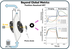
This study introduces position-resolved operando X-ray transmission as a powerful approach to track ion concentrations inside a working capacitive deionization (CDI) cell. The method resolves local ion changes along the flow channel and within individual nanoporous electrodes. It reveals strong spatial and flow-rate-dependent concentration gradients that are invisible to conventional effluent-based measurements. The results show that ion replenishment strongly limits charge efficiency at low flow rates, while ultramicropore-induced ionophobicity promotes counter-ion adsorption and enhances desalination performance. Overall, the study demonstrates how local operando X-ray diagnostics provide direct insight into ion transport and efficiency losses, enabling improved CDI material and cell design.
The research work was conducted from: Johannes Kepler University Linz, Austria; Technical University of Leoben, Austria; Joanneum Research mbH, Austria; Brno University of Technology, Czechia; and University of Pisa, Italy.
The Chair of Physics was responsible for the AFM analysis performed by B. Ban and C. Teichert.
The image represents the designer's view of a pincer-like robot device in the shape of a soldering iron controlled by a master bee employed to solder a PCB board covered in a beeswax encapsulate layer.
Many naturally occurring waxes, like beeswax represented here, are demonstrated by C.V. Irimia et al . to be excellent dielectrics for organic field effect transistors, aimed to reach sustainability in the electronics world.
Image partly generated using Adobe Firefly and reproduced
by permission of Johannes Kepler University Linz from
J . Mater . Chem . C , 2025, 13 , 14767.
Gennadiy Murastov, Awais Aslam, Simon Leitner, Aleksandar Matkovic 2D Mat Lab
We report two-dimensional WSe2 field-effect transistors with multi-layer palladium diselenide (PdSe2) as a contact material. We demonstrate that PdSe2 contacts favour hole injection while preserving the ambipolar nature of the channel material. This consequently yields high-performance p-type WSe2 devices with PdSe2 van der Waals contacts. Further, we explore the tunability of the contact interface by selective laser alteration of the WSe2 under the contacts, enabling pinning of the threshold voltage to the valence band of WSe2, yielding pure p-type operation of the devices.
This study reports on the applicability of X-ray transmission (XRT), small- and wide-angle X-ray scattering (SAXS/WAXS) and small-angle neutron scattering (SANS) for investigating fundamental processes taking place in the working electrode of an electric double-layer capacitor with 1 M RbBr aqueous electrolyte at different applied potentials. XRT and incoherent neutron scattering are employed to determine global ion- and water-concentration changes and associated charge-balancing mechanisms. We showcase the suitability of SAXS and SANS, respectively, to get complementary information on local ion and solvent rearrangement in nanoconfinement, but also underscore the limitations of simple qualitative models, asking for more quantitative descriptions of water–water and ion–water interactions via detailed atomistic modelling approaches
Electric Potential at the Interface of Membraneless Organelles Gauged by Graphene
Christian Hoffman, Gennadiy Murastov, Johannes Vincent Tromm, Muhammad Awais Aslam, Aleksandar Matkovic, Dragomir Milovanovic 2D_Mat_Lab
Eukaryotic cells contain membrane-bound and membrane-less organelles that are often in contact with each other. How the interface properties of membrane-less organelles regulate their interactions with membranes remains challenging to assess. Here, we employ graphene-based sensors to investigate the electrostatic properties of synapsin 1, a major synaptic phosphoprotein, either in a single phase or after undergoing phase separation to form synapsin condensates. Using these graphene-based sensors, we discover that synapsin condensates generate strong electrical responses that are otherwise absent when synapsin is present as a single phase. By introducing atomically thin dielectric barriers, we show that the electrical response originates in an electric double layer whose formation governs the interaction between synapsin condensates and graphene. Our data indicate that the interface properties of the same protein are substantially different when the protein is in a single phase versus within a biomolecular condensate, unraveling that condensates can harbor ion potential differences at their interface.
Gennadiy Murastov Muhammad Awais Aslam, Aleksandar Matkovic 2D Mat_Lab
Combining metallic nanoparticles and 2D semiconductors is a promising pathway to tailor hybrid mixed-dimentional plasmonic systems. However, current research focuses on either stacking nanopartiles on 2D layers or vice versa, commonly compromising electronic properties of the 2D materials due to perturbation of its basal plane. Here, we report a direct one-step controllable growth of silver nanoparticles along tungsten diselenide nanoribbon edges via edge-specific on-surface photochemistry for boosting light-matter coupling effect, optoelectronic response, and improving photocatalytic performance.
Probing Magnetic Ordering in Air Stable Iron-Rich Van der Waals Minerals
Muhammad Zubair Khan Oleg E. Peil Muhammad Awais Aslam Johann G. Raith 2DMat_Lab
2D Phyllosilicates bridge the gap between nanotechnology and mineralogy, revealing a novel class of 2D magnetic insulators. These minerals can incorporate substantial amount of local magnetic moment bearing ions with ambient stability. This paper demonstrates the relation between their structure and magnetic properties, offering insights into achieving higher critical ordering temperatures through oxidation state engineering.
M.V. Rauscher , Malina Seyfertitz J. Appl. Cryst. (2023). 56, 801-809 / SyNergy_Mat Lab
In situ small-angle X-ray scattering (SAXS) was employed to identify critical parameters during thermal treatment for template removal of an ordered mesoporous carbon precursor synthesized via a direct soft-templating route. The structural parameters obtained from the SAXS data as a function of time were the lattice parameter of the 2D hexagonal structure, the diameter of the cylindrical mesostructures and a power-law exponent characterizing the interface roughness. Moreover, detailed information on contrast changes and pore lattice order was obtained from analysis of the integrated SAXS intensity of the Bragg and diffuse scattering separately. Five characteristic regions during heat treatment were identified and discussed regarding the underlying dominant processes. The influence of temperature and O2/N2 ratio on the final structure was analyzed, and parameter ranges were identified for an optimized template removal without strongly affecting the matrix. The results indicate that the final structure and controllability of the process are optimum for temperatures between 260 and 300°C with a gas flow containing 2 mol% of O2.
Electrical monitoring of organic crystal phase transition using MoS2 field effect transistor
I. Boulet et.al. Nanoscale Advances 5, 1681–1690, 2023, 2D_Mat_Lab SPMG
Hybrid van der Waals heterostructures made of 2D materials and organic molecules exploit the high sensitivity of 2D materials to all interfacial modifications and the inherent versatility of the organic compounds. In this study, we are interested in the quinoidal zwitterion/MoS2 hybrid system in which organic crystals are grown by epitaxy on the MoS2 surface and reorganize in another polymorph after thermal annealing. By means of field-effect transistor measurements recorded in situ all along the process, atomic force microscopy and density functional theory calculations we demonstrate that the charge transfer between quinoidal zwitterions and MoS2 strongly depends on the conformation of the molecular film. Remarkably, both the field effect mobility and the current modulation depth of the transistors remain unchanged which opens up promising prospects for efficient devices based on this hybrid system. We also show that MoS2 transistors enable fast and accurate detection of structural modifications that occur during phases transitions of the organic layer. This work highlights that MoS2 transistors are remarkable tools for on-chip detection of molecular events occurring at the nanoscale, which paves the way for the investigation of other dynamical systems.
A comparison of small-angle scattering with electron microscopy techniques to characterize low volume fractions of heterogeneously distributed precipitates in alloys
Honaramooz, Mohammad Taha / SyNergy_Mat Lab
The characterization of Zr-containing dispersoids in aluminum alloys is challenging due to their broad size distribution, low volume fraction, and heterogeneous distribution within the grains. In this work, small-angle X-ray scattering (SAXS) and small-angle neutron scattering (SANS) were compared to scanning electron microscopy (SEM) and transmission electron microscopy (TEM) regarding their capability to characterize Zr-containing dispersoids in aluminum alloys. It was demonstrated that both scattering techniques are suitable tools to characterize dispersoids in a multiphase industrial aluminum alloy. While SAXS is more sensitive than SANS due to the high electron density of Zr, SANS has the advantage of being able to probe a much larger sample volume. The combination of SAXS and SANS allows for the verification that the dispersoids can be separated from other precipitate phases. The size distribution obtained from SAXS, SANS and TEM showed good agreement. The SEM-derived size distributions were, however, found to significantly deviate from those of the other techniques, which can be explained by considering the resolution-limited restrictions of the different techniques
Single Crystalline 2D Material Nanoribbon Networks for Nanoelectronics
Muhammad Awais Aslam / Matkovic's Lab
The last decade has seen a flurry of studies related to graphene nanoribbons owing to their potential applications in the quantum realm. However, little experimental work has been reported towards nanoribbons of other 2D materials due to the absence of synthesis routes. Here, we propose a universal approach to synthesize high-quality networks of nanoribbons from arbitrary 2D materials while maintaining high crystallinity, sufficient yield, narrow size distribution, and straight-forward device integrability. The wide applicability of this technique is demonstrated by fabricating MoS2, WS2, WSe2, and graphene nanoribbon field effect transistors that inherently do not suffer from interconnection resistances. By relying on self-assembled and self-aligned organic nanostructures as masks, we demonstrate the possibility of controlling the predominant crystallographic direction of the nanoribbon’s edges. Electrical characterization shows record mobilities and very high ON currents for various TMDCs despite extreme width scaling. Lastly, we explore decoration of nanoribbon edges with plasmonic particles paving the way towards the development of nanoribbon-based plasmonic sensing and opto-electronic devices.
A universal substrate for the nanoscale investigation of two-dimensional materials
T.H. Tran et.al., Applied Surface Science 604, 154585, 2022/ Matkovics Lab
Since discovering two-dimensional materials, there has been a great interest in exploring, understanding, and taking advantage of their unique properties. Si/SiO2 is one of the most used substrates for the deposition and characterization of 2D materials due to its availability and optical contrast. This work goes beyond the conventional substrate and introduces highly-ordered pyrolytic graphite (HOPG) as universal support for investigating two-dimensional materials due to several unique properties such as chemical and temperature stability, intrinsic high flatness, reusability, electrical conductivity, ease of use, availability, and enhanced adhesion of two-dimensional materials. We demonstrate this by analyzing several 2D materials with advanced atomic force microscopy methods, Raman and photoluminescence spectroscopy with hyperspectral imaging, and scanning electron microscopy with elementary analysis imaging. The strong adhesion to HOPG allowed the instant deposition of different two-dimensional materials GaSe, MoS2, Zn2In2S5, talc, and h-BN. This feat is hard to accomplish on the conventional SiO2 substrate without polymer-assisted transfer. Moreover, this strong interaction can strain 2D materials deposited on HOPG, giving localized changes in reactivity, optical, and electronic properties. This effect is explored for selective Ag deposition on strained regions of 2D materials to activate photocatalytic reactions.
Coffee Waste-Derived Nanoporous Carbons for Hydrogen Storage
Sebastian Stock ACS Applied Energy Materials / SyNergy_Mat Lab
Biological waste such as residues from the food and beverage industry provides a valuable and abundant resource to be used as a precursor for the synthesis of activated carbons that can be subsequently employed as adsorbents for, e.g., hydrogen storage. Materials with a large specific surface area and pores of appropriate size are necessary to achieve reasonable hydrogen adsorption capacity. Here, we present the repeatable synthesis of activated carbons from coffee waste, i.e., spent coffee grounds and coffee silver skins, on the basis of two independently synthesized batches. The carbonization process under nitrogen gas flow followed by chemical activation with solid potassium hydroxide results in microporous carbons with bimodal pore size distribution and specific surface area up to 3300 and 2680 m2/g based on Brunauer–Emmett–Teller and density functional theory methods, respectively. The materials exhibit excellent hydrogen adsorption performance under cryogenic conditions (77 K), reaching high and fully reversible excess gravimetric hydrogen uptake values of up to 5.79 wt % at 37 bar, and total capacities exceeding 9 wt % at 100 bar.

